The Manufacture and Parameter Choose of MOV Pieces Used in Voltage Limiting Type SPD
Fei Zi Hao1 Wang Zhi Hong1
Chen Ze Tong2 Liu Xi Hua2
1. Guizhou Flyboat Electronic co., Ltd
2. Comtech Communication Technology(Shen Zhen) Co.,Ltd.
Abstract: The difference of required properties between MOV pieces used in voltage limiting type SPD and general varister ware compared. The MOV pieces properties influenced by two type heat treatment process ware analyzed. Consider geometric form and internal stress differences, the point is that the reduction of silver electrode by quick heat and cool process does not fit for 34×34mm MOV pieces. The V-A curve of ZnO varister was studied, the point is that the non-linear coefficient(α) value of MOV pieces with big area between 0.1mA~1mA should not be too higher. The MOV pieces leak current and its dispersion was discussed combined with practical experience.
Key Word: Voltage limiting type SPD MOV pieces Non-linear coefficient Leak Current Internal stress.
Key words: pressure limiting type SPD MOV Chip Non-linear coefficient Leakage Stress
1. 1. Introduction
With the increasing requirements of the construction Lightning, Surge Protection Device (SPD) in building more and more widely on the application, has gradually become a low-voltage electrical appliances, an important part of a large-scale limit of pressure-type SPD is just around the corner into the home Most limit the use of pressure-type SPD is 34 × 34mm in ZnO varistor (MOV) chips. At present, some MOV and SPD manufacturing large-size enterprises are not fully aware of MOV varistor chips and the distinction between general-purpose, easy to general-purpose Varistor manufacturing process and the three-parameter measurement method for sorting SPD chip with MOV screening, SPD has seriously affected the quality of products, but also to the SPD user conceals potential problems. So, I feel a need for some understanding of this issue, combined with practical work, in this to make some introductory remarks.
2. 2. Universal varistor MOV and performance requirements of the main differences between
Pressure limiting the use of MOV-type SPD chip geometry large capacity for high-pass flow, residual pressure smaller than required. For example, 34 × 34mm chip demand 8 / 20 μ s Nominal Flow In 20kA, Imax 40kA / 2 times; and Φ 20 general-purpose Varistor Maximum Flow capacity of 10kA / 1 times; former instantaneous current density of 34.6A / mm 2, the latter 31.8A/mm 2, the two difference of 10%; the former is not required to undergo secondary damage, while the latter only once; the former SPD produced after the heat balance needed to withstand the test of (referring to the MOV chip flow, respectively 2mA -5A power frequency AC current), so the former char thermal capacity required to be much larger than the latter. As the large geometry, shape differences, electrical performance requirements of high, SPD chip manufacturing process with the MOV and electrical parameters on features has its particularity.
These two kinds of products focused on similarities and differences between the performance requirements of the following table:
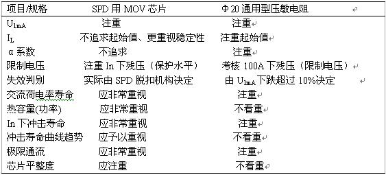
This focuses on what SPD chip with MOV heat capacity should pay attention to the reasons: SPD principle is the use of the heat from the MOV chip failure load after the role of frequency, its leakage current growing cause chip heating the heat from the body of the low melting point solder alloy melting point to cut off from the circuit to achieve the conservation purposes, MOV chip self-breakdown problems still exist in hot-melt, once the chip is hot-melt MOV breakdown, it becomes a low resistance conductor, causing the system short-circuit, sometimes from inside the arc to make the module the rapid gasification of the material, the pressure surge caused by an explosion, fire-breathing combustion, damaged equipment, and buildings. Therefore, heat from the body must breakdown in the MOV chip is achieved by hot-melt from the heat capacity of a large MOV chips breakdown before being hot-melt could insist on a longer time to ensure that heat from the body of the low melting point alloy solder melting point, namely should pay attention to MOV-chip thermal capacity reasons. On the same kinds of materials, the general only by increasing the material quality to increase heat capacity, in the case of a fixed radial size, only that the chip thickness increase the axial dimension to increase its thermal capacity; but the chip thickness also gives rise to the problem of the residual pressure is increased, so the performance requirements of the chip should be comprehensive and balanced, not too much emphasis on one.
3. 3. Chip geometry, size and process the relationship between the thermal process
Obvious difference due to the above, SPD Manufacturing Process with MOV chips also have a distinction between general-purpose Varistor. MOV chip manufacturing process with a few key processes are as follows: According to formula ingredients, mixing spray granulation → → Pressing → row rubber, sintering → heat burning silver electrode. Performance of the chip manufacturing process closely linked to their strengths and weaknesses of the current burning craft of silversmithing at the last one before the small differences in the various manufacturing processes, have their own strengths. Finally a craft there are two approaches: one is the reference to the current high-voltage surge arrester valve of the annealing process, using slow-burning heating and cooling will be merged into Bank and annealing process to complete a process in order to fully eliminate or reduce the chip's internal stress, the whole process about 25h or so to complete, so that leakage current out of the chip is usually larger, 34 × 34mm chip, is about 5 ~ 15 μ A; α coefficient of the lower, about 18 ~ 35. The other is the direct use of small varistors fast-fired silver production process, some tens of minutes to complete, some of this done before annealing, and some not do. This out of 34 × 34mm chip leakage current is usually ≤ 2 μ A; α coefficient ≥ 40. As most of SPD chip manufacturing plants are mainly the production of small varistors, this process has been widely used.
In the previous process guaranteed under the premise of a final heat treatment process of burning silver will greatly affect the performance of chips on the large size of the square chip in particular.A simple analysis is as follows: For the Φ 20 below in terms of a small wafer, because it is round, and the small size, thermal expansion and contraction caused by thermal process more uniform and the magnitude is small, the stress within the chip, most concentrated in the center of a circle near the Therefore, you can use the fast-burning craft of silversmithing. While the 34 × 34mm chip, since all the tracks and the large size ranges, thermal process caused by thermal expansion and contraction rate of large and uneven, rapid heating and cooling in the chip caused great stress, plus In the firing process on the thermal deformation stress. From the materials science we can see that too much stress will affect the phase change material inside, inhibit carrier movement so as to enhance grain, grain boundary resistance. Right MOV chip for the external manifestations U 1mA voltage rise, leakage current I L decreases, α increases the coefficient, it seems that small current performance is improved. But this is only the illusion of a non-steady state, with the release of internal stress, electrical performance will be faster deterioration; and because of the increase of resistance, will reduce the 8 / 20 μ S Flow capacity, life expectancy curve of apparent sudden change of performance (U 1mA to withstand a certain number of values in the impact of a sharp decline after), small current characteristics significantly worse (I L increased, α coefficient decreased rapidly); conducting 2mS square-wave energy test easier to breakdown, making 8 / 20 are susceptible to limit the impact of burst phenomena (surge of energy and stress of the structure of ceramics produced at the same time destroyed). If the stress release process, including frequency associated with the role of the external electric field, the impact mechanism is more complex, but the result is that chip performance, accelerated aging. Therefore must not be general-purpose Varistor copied the rapid firing technology to large square silver MOV chip production.
Practice the craft was found that if after full annealing chip (U 1mA = 600 ~ 620V, I L = 8 μ A ±, α = 23 ±) melted down the fast simulation of 600 ℃ burn silver, its performance will undergo significant changes in : V 1mA ≥ 660V, I L ≤ 2, α ≥ 40, but 8 / 20 μ S Limit Flow capacity and 2mS square energy tolerance decreased, so the first heat treatment process and then quickly burn silver no practical significance. In this regard should draw on-chip high-voltage surge arrester annealing process and control targets, from the silver paste to improve the quality of start, will burn silver and merged into a heat-treatment process, in order to eliminate or reduce the chip stress.
4. 4Small current parameter selection should pay attention to several issues
A typical ZnO varistor voltage-current characteristic curves of the following diagram shows an example,
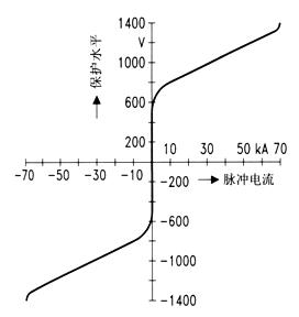
Shui Po, there is a clear fold, usually defined 1cm
2 chips 1mA current flow when the voltage
U 1mA/cm
2 for the knee voltage
[1], also known as the breakdown voltage or breakdown voltage. When the voltage applied on-chip voltage below the inflection point, the voltage and current near-linear relationship, this time a smaller non-linear coefficient α; Once the role of the on-chip voltage exceeds the inflection point voltage, the voltage will be a small increment led to a sharp increase in current, voltage and current meter emerged in a strong non-linear relationship, this time have a high nonlinear coefficient α. It is emphasized that the small size of general-purpose pressure-sensitive resistor, the varistor voltage U
1mA can be approximated as the inflection point voltage
U 1mA/cm
2; and if ignored the impact of the thickness uniformity, 34 × 34mm chip, is the U
10mA inflection point voltage
U 1mA/cm
2, U
1mA equivalent to only U
0.1mA / cm 2, nonlinear coefficient α = 1/lg (U
1mA / U
0.1mA) in fact is characterized by
U 0.01mA/cm
2 to U
0.1mA/cm 2 within the non-linear characteristics, we can see from the foregoing, this time turning point voltage is still below its α value should not be large; if forced through the heat treatment raise the value of this α can be interpreted as the upper half curve left shift occurred, it will certainly affect their ability to large currents flow passage. Based on actual experience, we recommend the α value should be controlled at between 20 to 35. Or directly under the provisions of a few current limit voltage to a more accurate description of the entire curve.
Leakage current I L is usually defined as 75% U 1mA under the conduction current, it is characterized by a low electric field area of the conductive properties of silicon, reflecting the grain boundary carrier high and low activation energy barrier. Its value is smaller, then expressed the need for greater energy to activate the grain boundary carrier. If I L is too small, the activation energy required is too large is doing 8 / 20 μ S limit-pass flow and 2mS square test prone to burst of energy. A confusing problem is the decentralized nature of leakage current, if I L in the 0.3 ~ 1.3 range that its dispersion is small; but if I L within 3 to 13, then that its great dispersion. In practice, we found that after heat treatment the increase of leakage current is basically proportional to, in other words the dispersion of the two is the basic equivalent. For the 34 × 34mm chip, we recommend the following in accordance with 75% U 1mA leakage flow of about 4 ~ 13 μ A control, both the general criteria used to meet domestic requirements, but also ensuring that the chip has good overall performance.
With the increase in valve geometry (multi-chip parallel), U 1mA / U 0.1mA reduction of α, I L increases, but because of non-linear characteristics, both change and area of not proportional.
Varistor in parallel use is a relatively large controversial issue. From the electrical performance point of view, a different varistor Despite certain differences, through appropriate selection of parameters can be used in parallel, but the means to achieve the parallel critical, if the means of properly, then fine selection of no significance of the parameters. In the main case should be considered high-frequency pulse current skin effect on both flow impact (and parameter selection is almost nothing to do), but also should consider the safety of thermal protection agencies from the backup problems. Recommended the adoption of the external circuit in parallel, each one located parallel independent fail-safe institutions. Do not think that multi-chip-chip direct welded together in parallel manner, due to multi-chip welded together, as lightning chip is good heat conductor, is likely to arise in which one has expired, but most of the heat generated by other welding with chips to absorb heat from the agencies failed to low melting point solder melting point, resulting in puncture frequency chips have been, as mentioned above will leave a serious accidents.
5. 5.Conclusion
From the use of environmental terms, SPD is usually installed in the distribution transformer (with high-voltage surge arrester) to the protected equipment (with a small pressure-sensitive resistors), with the section of the electrical environment is very complex and difficult; from the chip geometry point of view, commonly used 34 × 34mm chip size even more than the distribution based on the commonly used high-voltage surge arrester Φ 32 chip, but due to the use of low-voltage systems, the chip thickness and general quite small varistors; from the use of standard terms [2 ] [3], SPD chip performance requirements is also part of the combination of the two high, so SPD chip manufacturing process should also be integrated both. It should be in accordance with standard requirements, refer to large international companies advanced product samples, combined with high-voltage surge arresters and small chip varistors MOV indicators requires the establishment of SPD chip product-specific performance requirements of the industry or national standards. MOV chip during selection, it should be for its manufacturing process and is equipped with a proper understanding of electrical performance parameters to make the right request, to avoid the occurrence of hidden dangers; chip makers have an obligation to correct interpretation of the user in order to jointly promote the cause of lightning protection healthy development.
References
1. 1.Wu Han. Metal oxide nonlinear resistance characteristics and application of Tsinghua University Press, 1998.11.
2. 2. GB 18802. 1-2002 - 2002/IEC 61643-1: 1998, Low Voltage Distribution System Surge Protection Device (SPD) Part 1: Performance requirements and test methods.
3. 3. YD/T1235. 1-2002: Communications Office (stations) low-voltage distribution systems Surge protectors technical requirements